
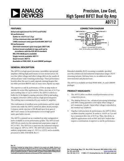
The AD712 dual op‑amp delivers high performance at modest cost, offering low input offset voltage, low drift, and a 16 V/µs minimum slew rate. It is suited for DAC/ADC buffers, active filters, photodiode preamps and other high‑speed analog applications.
The device is available in PDIP, SOIC_N and CERDIP packages, supports supply voltages up to ±18 V, and meets a range of temperature specifications from commercial to military grades. Detailed electrical specifications, typical performance curves and application notes are provided in the following sections.
| Input offset voltage (typical) | 1.0 mV |
|---|---|
| Slew rate (minimum) | 16 V/µs |
| Unity‑gain bandwidth (minimum) | 3 MHz |
| Open‑loop gain (minimum) | 200 V/mV |
| Maximum supply voltage rating | ±18 V |
The AD712 has a minimum slew rate of 16 V/µs.
Typical input offset voltage is 1.0 mV.
The AD712 is available in 8‑lead PDIP, SOIC_N and CERDIP packages.
The device is rated for a maximum supply voltage of ±18 V.