
This datasheet provides details about the LT6220/LT6221/LT6222's features, including low voltage, high frequency signal processing, driving A/D converters, rail-to-rail buffer amplifiers, active filters, video amplifiers, fast current sensing amplifiers, etc.
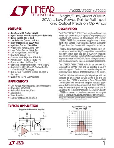
The LT6220/LT6221/LT6222 family provides single, dual, and quad precision operational amplifiers with rail‑to‑rail input and output capability. Key features include a 60 MHz gain‑bandwidth product, low quiescent current (1 mA max), input offset voltage as low as 350 µV, and a wide supply range of 2.2 V to 12.6 V. These devices are suited for low‑voltage, high‑frequency signal processing, A/D converter driving, rail‑to‑rail buffering, active filters, video amplification, and fast current‑sensing applications.
Available in 8‑pin SO, 5‑pin ThinSOT, 8‑pin DFN, and 16‑pin SSOP packages, the amplifiers deliver up to 50 mA typical output current. Detailed electrical characteristics cover input offset voltage, bias current, common‑mode rejection, power‑supply rejection, slew rate, and temperature ranges, ensuring reliable performance from –40 °C to 85 °C.
| Gain‑Bandwidth Product | 60 MHz |
|---|---|
| Input Offset Voltage (max) | 350 µV |
| Input Bias Current (max) | 150 nA |
| Supply Voltage Range | 2.2 V to 12.6 V |
| Typical Output Current | 50 mA |
| Slew Rate (typ) | 20 V/µs |
| Power Supply Rejection Ratio (typ) | 105 dB |
| Common Mode Rejection Ratio (typ) | 102 dB |
| Operating Temperature Range | –40 °C to 85 °C |
The devices operate from 2.2 V up to 12.6 V supply voltage.
Each amplifier can source or sink up to 50 mA typical output current.
The LT6220 is offered in an 8‑pin SO package and a 5‑pin ThinSOT™ package.
The input offset voltage is specified as 350 µV maximum (typical 70 µV).