
Low noise boost converters with integrated power switch, Schottky diode and output disconnect circuitry
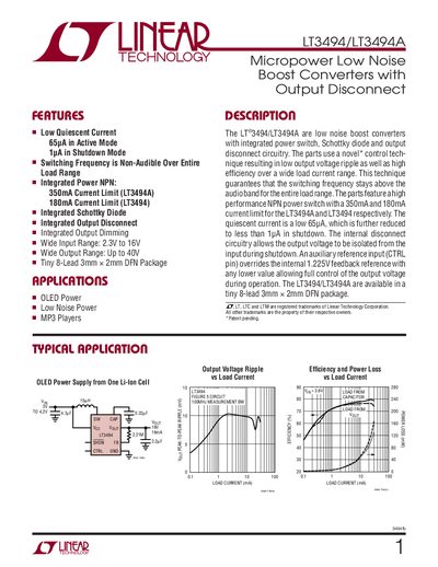
This manual describes the LT3494 and LT3494A micropower low‑noise boost converters with integrated power switch, Schottky diode, and output‑disconnect circuitry. It lists key features such as low quiescent current, non‑audible switching frequency, wide input (2.3 V‑16 V) and output ranges, and integrated dimming capability.
The document provides absolute maximum ratings, package dimensions, pin descriptions, electrical characteristics, and design guidance for inductors, capacitors, and feedback networks. Application notes, typical performance curves, and example circuits are included to help designers implement the devices in OLED power supplies, MP3 players, and other low‑power applications.
| Minimum Operating Voltage | 2.3 V |
|---|---|
| Maximum Operating Voltage | 16 V |
| Feedback Voltage (typical) | 1.225 V |
| Quiescent Current (Not Switching) | 65 pA |
| Quiescent Current (Shutdown) | 0‑1 pA |
| Switch Current Limit (LT3494A) | 350 mA |
| Switch Current Limit (LT3494) | 180 mA |
| Maximum Switch Off Time | 30 µs |
The quiescent current in the non‑switching state is specified as 65 pA.
The LT3494A version has a typical peak current limit of 350 mA.
The device operates from 2.3 V up to 16 V input.