
TLC5620C and TLC5620I are quadruple 8-bit voltage output digital-to-analog converters (DACs) with buffered reference inputs (high impedance).
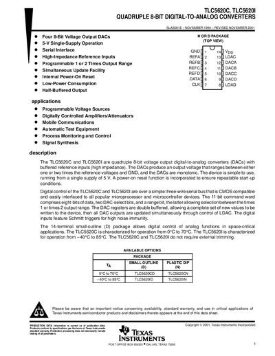
The TLC5620C and TLC5620I are quadruple 8‑bit voltage‑output digital‑to‑analog converters (DACs) with buffered high‑impedance reference inputs. They operate from a single 5 V supply, provide programmable 1× or 2× output range, and feature a simultaneous update facility via the LDAC pin. The devices are designed for space‑critical applications such as programmable voltage sources, signal synthesis, and automatic test equipment.
The datasheet includes functional block diagrams, pin descriptions, recommended operating conditions, electrical characteristics, mechanical dimensions, and an important notice on warranty and product availability. Key performance parameters such as supply voltage range, input voltage thresholds, reference voltage, and timing specifications are detailed for designers.
| Supply voltage (Vpp) | 4.75 V – 5.25 V |
|---|---|
| High‑level input voltage (VIH) | 0.8 Vpp |
| Low‑level input voltage (VIL) | 0.8 Vpp |
| Reference voltage (Vref) | Vpp ‑ 1.5 V |
| Analog full‑scale output voltage | 3.5 V (RL = 10 kΩ) |
| Load resistance | 10 kΩ |
| Pulse duration LOAD | 250 ns |
| Clock frequency | 1 MHz |
The recommended supply voltage (Vpp) is 4.75 V to 5.25 V.
The device contains four independent 8‑bit DAC channels (DACA, DACB, DACC, DACD).
The maximum clock frequency is 1 MHz.
High‑level input voltage (VIH) is 0.8 Vpp and low‑level input voltage (VIL) is 0.8 Vpp.