
The AT26DF321 is a serial interface Flash memory device designed for use in a wide variety of high-volume consumer based applications in which program code is shad- owed from Flash memory into embedded or external RAM for execution. The flexible erase architecture of the AT26DF321, with its erase granularity as small as 4-Kbytes, makes it ideal for data storage as well, eliminating the need for additional data storage EEPROM devices. The physical sectoring and the erase block sizes of the AT26DF321 have been opti- mized to meet various application requirements.
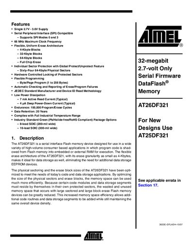
This document provides a complete description of the AT26DF321 serial flash memory, including its operating voltage range, SPI interface, and flexible erase architecture. It explains the device’s sector and block organization, protection mechanisms, and programming capabilities.
The datasheet also contains pin descriptions, timing diagrams, command tables, and errata information, along with contact details for Atmel technical support.
| Supply Voltage | 2.7 V – 3.6 V |
|---|---|
| Maximum Clock Frequency | 66 MHz |
| Erase Block Sizes | 4 KB, 32 KB, 64 KB, Full Chip |
| Number of Physical Sectors | 64 × 64 KB |
| Active Read Current (typical) | 7 mA |
| Deep Power‑Down Current (typical) | 4 µA |
| Endurance | 100 000 Program/Erase Cycles |
| Data Retention | 20 Years |
| Package Options | 8‑lead SOIC (200‑mil) and 16‑lead SOIC (300‑mil) |
The device operates from 2.7 V to 3.6 V.
Up to 256 bytes can be programmed in one Byte/Page Program operation.
It offers individual sector protection, global protect/unprotect, and hardware‑controlled lock pins.
The memory can be erased in 4 KB, 32 KB, 64 KB blocks, or a full‑chip erase.