
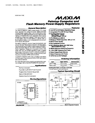
This manual provides a general description of the MAX717‑MAX721 CMOS power‑supply ICs, which generate dual regulated DC outputs for palmtop computers, flash‑memory/PCMCIA power supplies, and portable data‑collection equipment. It outlines the device features such as low‑voltage battery operation, high switching frequency, and efficient power conversion.
The document includes pin configurations, absolute maximum ratings, electrical characteristics, typical operating curves, and detailed pin descriptions. It also covers the pulse‑frequency modulation control scheme, evaluation‑kit component placement, and ordering information for the various device variants.
| Battery Operating Range | 0.9 V to 5.5 V |
|---|---|
| Unregulated Input Voltage Range | 7 V to 20 V DC |
| Main Output Voltage Options | 3.3 V or 5 V (selectable) |
| Auxiliary Output Voltage Options | 5 V or 12 V (selectable) |
| Maximum Switching Frequency | 500 kHz |
| Efficiency at 200 mA Load | 87 % |
| Quiescent Current | ≈ 60 µA |
The device accepts an unregulated DC input voltage from 7 V to 20 V.
The main output can be set to 3.3 V or 5 V, and the auxiliary output can be set to 5 V or 12 V.
The regulator can switch at up to 500 kHz.
The quiescent current is approximately 60 µA.