
LM1882•54ACT715 LM1882-R•54ACT715-R are programmable video sync generators capable of generating Horizontal, Vertical and Composite Sync and Blank signals for televisions and monitors. All pulse widths are completely definable by the user. The devices are capable of generating signals for both interlaced and noninterlaced modes of operation. Equalization and serration pulses can be introduced into the Composite Sync signal when needed. Four additional signals can also be made available when Composite Sync or Blank are used. These signals can be used to generate horizontal or vertical gating pulses, cursor position or vertical Interrupt signal. These devices make no assumptions concerning the system architecture. Line rate and field/frame rate are all a function of the values programmed into the data registers, the status register, and the input clock frequency. The ’ACT715/LM1882 is mask programmed to default to a Clock Disable state. Bit 10 of the Status Register, Register 0, defaults to a logic “0”. This facilitates (re)programming before operation. The ’ACT715-R/LM1882-R is the same as the ’ACT715/ LM1882 in all respects except that the ’ACT715-R/ LM1882-R is mask programmed to default to a Clock Enabled state. Bit 10 of the Status Register defaults to a logic “1”. Although completely (re)programmable, the ’ACT715-R/ LM1882-R version is bet
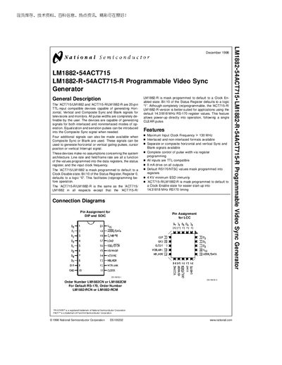
The LM1882 (ACT715) and LM1882‑R (ACT715‑R) are 20‑pin TTL‑compatible devices that generate horizontal, vertical and composite sync and blank signals for televisions and monitors. All pulse widths are fully programmable via internal registers, and the devices support both interlaced and non‑interlaced video formats. Four additional signals can be derived for gating, cursor positioning, or vertical interrupt functions.
The datasheet details the pin assignments, register map, timing calculations, and programming procedures. It also describes the default mask‑programmed states, clock enable/disable behavior, and special features such as scan mode for non‑destructive register verification.
| Maximum Input Clock Frequency | > 130 MHz |
|---|---|
| Minimum ESD Immunity | 4 kV |
| Output Drive Capability | 8 mA on all outputs |
| Default RS‑170/NTSC Values | Mask‑programmed into registers |
| Number of Inputs | 13 |
| Number of Outputs | 5 |
The ACT715‑R/LM1882‑R is mask programmed to default to a Clock Enabled state.
The device provides 13 inputs and 5 outputs.
The CLEAR pin is an asynchronous input that initializes the device when it is HIGH, resetting all registers to their mask‑programmed values.