
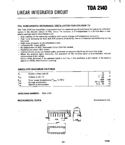
The TDA 2140 is a monolithic linear integrated circuit designed to regenerate and process the sub‑carrier reference signals in PAL colour‑TV receivers. It is supplied in a 16‑lead dual‑in‑line plastic package and provides a stable oscillator, high noise immunity, an integrated 90° phase shifter and automatic colour‑killer control.
The document lists absolute maximum ratings, mechanical dimensions, electrical characteristics such as supply voltage (10.8‑13.2 V), supply current (64 mA typical) and pin‑by‑pin functions, as well as application information for connecting the device in a TV decoder circuit.
| Supply current (I) | 64 mA typical |
|---|---|
| Ref. (B‑Y) output voltage (peak‑to‑peak) | 0.9 V |
| Maximum flyback pulse amplitude | 55 Vpp |
| Thermal resistance (junction‑ambient) | 100 °C·W⁻¹ max |
Pin 9 provides the output of the colour‑killer circuit, which activates when the antenna signal is too low or the oscillator is not locked.
The absolute maximum rating for the supply voltage on pin 2 is 15 V.
The flyback pulse must be negative with a maximum amplitude of 55 Vpp.