
Key facts
- Brand
- TDA
- Model
- TDA 2140
- Category
- Other Electronics
- Industry
- Electronics
- Documents
- 2
- Languages
- EN
- Last added
- 2012-04-01
Start here
TDA 2140 Integrated Circuit Manual
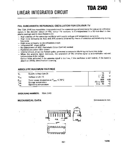
This document describes the TDA 2140 monolithic integrated circuit used for regenerating and processing the subcarrier reference signals in PAL colour TV receivers. It includes the main features, absolute maximum ratings, mechanical dimensions, and a block diagram of the circuit.
Detailed pin‑by‑pin information, electrical characteristics, and application notes are provided, covering supply voltage, current consumption, output waveforms, colour‑killer operation, and the automatic phase‑control circuit.
TDA 2140 specifications
| Supply current (I) | 64 mA typical |
|---|---|
| Ref. (B‑Y) output voltage (peak‑to‑peak) | 0.9 V |
| Maximum flyback pulse amplitude | 55 Vpp |
| Thermal resistance (junction‑ambient) | 100 °C·W⁻¹ max |
All TDA 2140 documents by type
Ratings, dimensions and ordering codes, for selection and design work.
Questions answered in these manuals
What does pin 9 do?
Pin 9 is the colour‑killer output, which is activated when the antenna signal is too low or the oscillator is not locked.
How is the sandcastle pulse generated?
The sandcastle pulse is taken from the flyback pulse applied at pin 15 and shaped by the RC network connected to pin 14.
What does pin 9 do?
Pin 9 provides the output of the colour‑killer circuit, which activates when the antenna signal is too low or the oscillator is not locked.
What is the maximum allowable supply voltage?
The absolute maximum rating for the supply voltage on pin 2 is 15 V.