
The document introduces the ADM202/ADM203, which is a high-speed, +5 V, 0.1 �F CMOS RS-232 driver/receiver pair. It features single supply +5 V operation, high efficiency, and +5 V to +10 V voltage doubler.
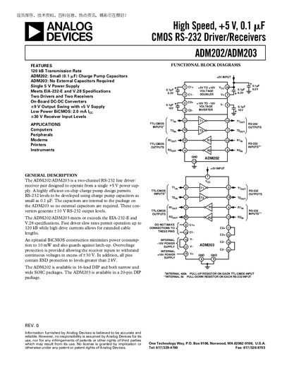
The ADM202 and ADM203 are two‑channel RS‑232 line driver/receiver pairs that operate from a single +5 V supply. The ADM202 uses small external 0.1 µF charge‑pump capacitors, while the ADM203 integrates the capacitors internally, eliminating the need for external parts. Both devices meet EIA‑232‑E and V.28 specifications and support data rates up to 120 kB.
The document includes detailed specifications, pin‑out diagrams, functional block diagrams, and typical performance curves. It also describes the internal charge‑pump voltage converter, transmitter and receiver sections, and provides mechanical dimensions for the available DIP and SOIC packages.
| Power Supply Current | 1.5 mA (no load) |
|---|---|
| Input Logic Threshold Low | 0.8 V |
| RS‑232 Input Voltage Range | -30 V to +30 V |
| Propagation Delay | 0.5 µs |
| Instantaneous Slew Rate | 25‑30 V/µs |
| Storage Temperature Range | ‑65 °C to +150 °C |
Both devices operate from a single +5 V power supply.
The ADM202 requires small external 0.1 µF charge‑pump capacitors, while the ADM203 has the capacitors built in and needs none.
They support transmission rates up to 120 kB.