
This document describes the features and characteristics of products in TSSOP package type, including the usage methods, functions, and power consumption of different instructions.
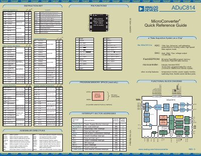
The ADuC814 MicroConverter Quick Reference Guide gives developers a concise overview of the device’s architecture, including the 8052‑compatible core, programmable PLL, and on‑chip peripherals. It lists the complete instruction set, pin assignments, interrupt vectors, and special function registers needed for low‑level programming.
Key features highlighted are a 12‑bit ADC with six channels, dual 12‑bit DACs, 8 KB Flash/EE program memory, 640 B data memory, 256 × 8 b user RAM, 16 I/O lines, temperature and power‑supply monitors, and a watchdog timer. The guide also shows the functional block diagram and memory map for quick reference during hardware design and firmware development.
| ADC resolution | 12‑bit |
|---|---|
| DAC resolution | dual 12‑bit |
| Flash program memory | 8 KB |
| Flash data memory | 640 B |
| User RAM | 256 × 8 bits |
| I/O lines | 16 |
| PLL clock range | 131 kHz – 16 MHz |
| Temperature monitor | present |
| Power‑supply monitor | present |
| Watchdog timer | present |
The ADuC814 includes a 12‑bit analog‑to‑digital converter.
The device provides 16 general‑purpose I/O lines.