
The document describes the instruction set and functionality of a specific product. It provides detailed descriptions of various operation instructions of the product, such as addition, subtraction, logical operations, etc. It also introduces the product's register and stack operations, as well as jump and conditional jump instructions. The product has efficient computation capabilities and flexible programming features.
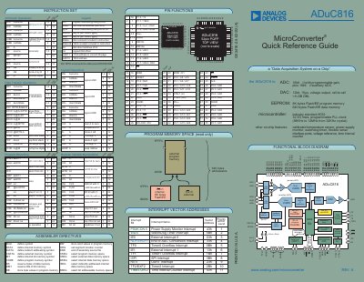
The ADuC816 Quick Reference Guide provides a concise overview of the MicroConverter's architecture, including its 8052‑core CPU, memory organization, and on‑chip peripherals. It is intended for engineers who need fast access to instruction encodings, register definitions, and pin functions.
Key sections cover the instruction set, interrupt vector table, functional block diagram, pin‑function tables, and detailed register maps. The guide also lists the device's built‑in ADC, DAC, watchdog timer, and serial interfaces, making it a handy reference during firmware development and hardware debugging.
| Program memory | 8 K bytes Flash/EE |
|---|---|
| Data memory | 640 bytes Flash/EE |
| Internal RAM | 8 K bytes |
| ADC | 16‑bit ΣΔ (primary) + 16‑bit ΣΔ auxiliary |
| DAC | 12‑bit, rail‑to‑rail |
| I/O lines | 32 programmable I/O pins |
The device provides 8 K bytes of Flash/EE program memory.
It has 32 programmable I/O lines.
It includes a 16‑bit ΣΔ ADC as the primary converter and an auxiliary 16‑bit ΣΔ ADC.
The on‑chip DAC is 12‑bit with rail‑to‑rail output.