
The AD767 is a complete voltage output 12-bit digital-to-analog converter including a high stability buried Zener reference and input latch on a single chip. The converter uses 12 precision high-speed bipolar current steering switches and a laser-trimmed thin-film resistor network to provide high accuracy. Microprocessor compatibility is achieved by the on-chip latch. The design of the input latch allows direct interface to 12-bit buses. The latch responds to strobe pulses as short as 40 ns, allowing use with the fastest available microprocessors. The functional completeness and high performance of the AD767 result from a combination of advanced switch design, high-speed bipolar manufacturing process, and the proven laser wafer-trimming (LWT) technology. The subsurface (buried) Zener diode on the chip provides a low-noise voltage reference which has long-term stability and temperature drift characteristics comparable to the best discrete reference diodes. The laser trimming process which provides the excellent linearity i
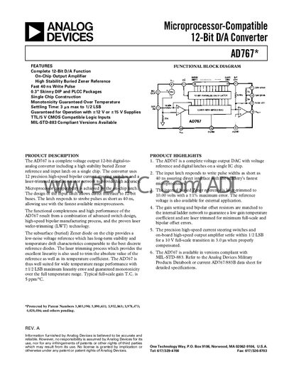
The AD767 provides a complete 12‑bit digital‑to‑analog conversion solution with a buried Zener reference, on‑chip output amplifier, and high‑speed bipolar switches. It supports TTL/5 V CMOS compatible logic inputs and can operate from +12 V or +15 V supplies, offering monotonic performance over the full temperature range.
The device is available in DIP, PLCC and ceramic packages, with specifications such as 12‑bit resolution, 3 ps settling to ½ LSB, 5 mA output current, and operation from –55 °C to +125 °C. Detailed timing, absolute maximum ratings, and grounding recommendations are provided for optimal high‑speed microprocessor interfacing.
| Resolution | 12 bits |
|---|---|
| Settling Time | 3 ps max to ½ LSB |
| Supply Voltage | +12 V or +15 V |
| Output Current | 5 mA |
The input latch responds to write pulse widths as short as 40 ns.
The AD767 settles to ½ LSB in as little as 3 ps.
The AD767 provides 12‑bit resolution.