
The AD7840 is a fast, complete 14-bit voltage output D/A converter. It consists of a 14-bit DAC, 3V buried Zener reference, DAC output amplifier, and high-speed control logic. The part features double-buffered interface logic with a 14-bit input latch and 14-bit DAC latch. Data is loaded to the input latch in either of two modes, parallel or serial. This data is then transferred to the DAC latch under control of an asynchronous LDAC signal. A fast data setup time of 21ns allows direct parallel interfacing to digital signal processors and high-speed 16-bit microprocessors. In the serial mode, the maximum serial data clock rate can be as high as 6MHz. The analog output from the AD7840
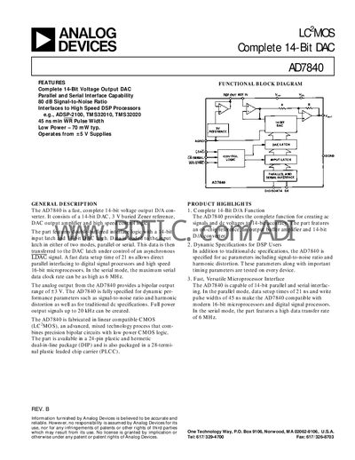
The AD7840 provides a complete 14‑bit D/A conversion function with both parallel and serial interface capabilities. It operates from a +5 V supply, draws about 70 mW typical power, and delivers a bipolar analog output range of ±3 V. The device includes an on‑chip 3 V temperature‑compensated Zener reference capable of sourcing up to 500 µA, and it is available in 24‑pin DIP, hermetic dual‑in‑line and 28‑pin PLCC packages.
Key performance figures include a minimum signal‑to‑noise ratio of 76 dB (typical 82 dB), total harmonic distortion of –78 dB max, and a fast 45 ns minimum write pulse width. Timing specifications allow a 21 ns data setup time for parallel operation and up to 6 MHz serial clock rate. The output buffer can drive 2 kΩ / 100 pF loads up to 6 Vpp and settles within 2.5 µs.
| Resolution | 14 bits |
|---|---|
| Typical SNR | 82 dB |
| Power Dissipation (max) | 100 mW |
| Typical Power Consumption | 70 mW |
| Supply Voltage | +5 V |
| Output Voltage Range | ±3 V |
| Maximum Serial Clock Rate | 6 MHz |
The minimum WR pulse width is 45 ns.
The device can operate with a serial clock up to 6 MHz.
Typical power consumption is about 70 mW.