
The AD7927 is a 12-bit, high speed, low power, 8-channel, successive approximation ADC with a sequencer. It features fast throughput rate, low power consumption, wide input bandwidth, and flexible power/serial clock speed management.
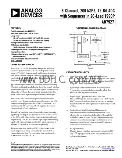
The AD7927 is a high‑speed, low‑power, 12‑bit successive‑approximation ADC that operates from a single 2.7 V to 5.25 V supply. It provides eight single‑ended inputs with a programmable channel sequencer and supports SPI, QSPI, Microwire and DSP‑compatible serial interfaces.
The device offers a maximum throughput of 200 kSPS, conversion times as short as 800 ns with a 20 MHz serial clock, and shutdown modes that reduce power draw to sub‑nanowatt levels. Detailed specifications, pin configurations, timing diagrams, and absolute maximum ratings are provided for designers.
| Resolution | 12 Bits |
|---|---|
| Maximum Throughput Rate | 200 kSPS |
| Conversion Time (20 MHz SCLK) | 800 ns |
| Power Consumption (3 V, 200 kSPS) | 3.6 mW max |
| Power Consumption (5 V, 200 kSPS) | 7.5 mW max |
| Input Bandwidth (Full‑Power) | 8.2 MHz @3 dB |
| Operating Temperature Range | -40 °C to +85 °C |
The AD7927 can sample up to 200 kSPS.
Conversion time is 800 ns (16 SCLK cycles) when the serial clock is 20 MHz.
Maximum power dissipation is 3.6 mW at 200 kSPS with a 3 V supply.
Input range can be 0 V to REFin or 0 V to 2 × REFin, selectable via the RANGE bit.