
The document is the data sheet for AD9467 Rev. C, which describes the features and characteristics of a 16-bit, 200 MSPS/250 MSPS analog-to-digital converter.
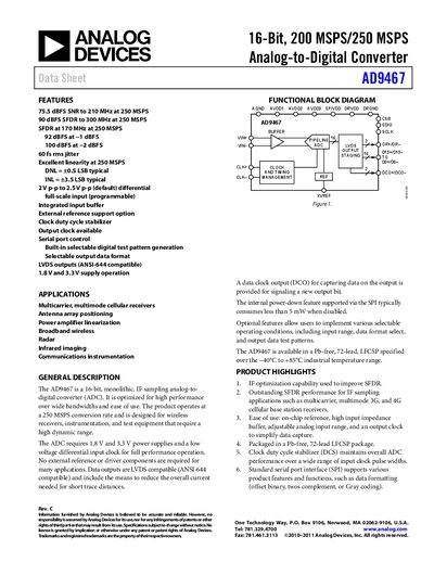
The AD9467 is a 16‑bit, 200 MSPS/250 MSPS analog‑to‑digital converter optimized for high‑performance, wide‑bandwidth applications such as wireless receivers and instrumentation. It operates from 1.8 V and 3.3 V supplies and provides LVDS‑compatible outputs with built‑in digital test pattern generation.
The document includes a functional block diagram, detailed pin descriptions, electrical and thermal specifications, and recommended PCB layout guidelines. It also lists ordering options for the 72‑lead LFCSP package and provides register maps for SPI configuration.
| Resolution | 16 bits |
|---|---|
| Maximum Sampling Rate | 250 MSPS |
| Full‑Scale Input Voltage | 2.5 V p‑p differential |
| Analog Supply Voltages | AVDD1 1.8 V, AVDD2 3.3 V, AVDD3 1.8 V |
| Digital Supply Voltage | DRVDD 1.8 V |
The AD9467 can sample at up to 250 MSPS.
It requires AVDD1 = 1.8 V, AVDD2 = 3.3 V, AVDD3 = 1.8 V for analog sections and DRVDD = 1.8 V for digital output drivers.
The device accepts a 2.5 V p‑p differential input.
Typical SNR is about 75 dBFS at 250 MSPS.