
TP3070, TP3071, TP3070-X COMBO® II Programmable PCM CODEC/Filter is a second-generation combined PCM CODEC and Filter device optimized for digital switching applications on subscriber line and trunk cards. Using advanced switched capacitor techniques, COMBO II combines transmit bandpass and receive lowpass channel filters with a companding PCM encoder and decoder. The devices are A-law and µ-law selectable and employ a conventional serial PCM interface capable of being clocked up to 4.096 MHz. A number of programmable functions may be controlled via a serial control port. Channel gains are programmable over a 25.4 dB range in each direction, and a programmable filter is included to enable Hybrid Balancing to be adjusted to suit a wide range of loop impedance conditions. Both transformer and active SLIC interface circuits with real or complex termination impedances can be balanced by this filter, with cancellation in excess of 30 dB being readily achievable when measured across the passband against standard test termination networks. To enable COMBO II to interface to the SLIC control leads, a number of programmable latches are included; each may be configured as either an input or an output. The TP3070 provides 6 latches and the TP3071 5 latches.
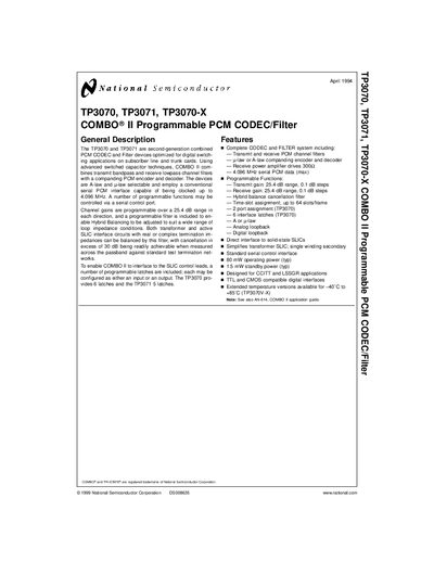
The COMBO II devices combine transmit and receive PCM channel filters with a selectable µ‑law or A‑law companding encoder and decoder. They support a serial PCM interface up to 4.096 MHz and provide programmable gain, hybrid balance, and time‑slot assignment functions.
The manual details pin descriptions, functional operation, power‑up/down sequences, programmable registers, and interface latch configuration, along with timing and clocking requirements for integration into subscriber line and trunk card applications.
| Maximum serial PCM data rate | 4.096 MHz |
|---|---|
| Receive power amplifier load | 300 Ω |
| Typical operating power | 80 mW |
| Typical standby power | 1.5 mW |
| Operating temperature range (TP3070‑X) | −40 °C to +85 °C |
| Number of interface latches (TP3070) | 6 |
| Number of interface latches (TP3071) | 5 |
The devices support a serial PCM data rate up to 4.096 MHz.
The TP3070 provides six interface latches.
The TP3070‑X version operates from –40 °C to +85 °C.