
S3C44B0X Chinese Datasheet, introduces the S3C44B0X memory controller characteristics, including little/big endian, bus width, start address, size, operation cycle, wait state, etc.
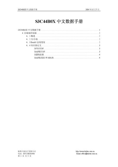
The document provides an overview of the S3C44B0X internal memory controller, describing its address space of 32 MB per bank (total 236 MB across 8 banks) and the ability to select little‑ or big‑endian mode via the ENDIAN pin. It also explains that each bank’s bus width is programmable to 8, 16 or 32 bits using the OM[1:0] pins.
Detailed register definitions are given for BWSCON, BANKCON, REFRESH and BANKSIZE, including bit fields for bus width, wait states, page mode, and DRAM refresh control. The register tables show how to configure memory types (ROM, SRAM, FP‑DRAM, EDO‑DRAM, Sync‑DRAM) and timing parameters such as Tacs, Tcos, Tacc, and others. This manual is written in Chinese.
| Address space per bank | 32 MB |
|---|---|
| Total address space | 236 MB across 8 banks |
| Number of memory banks | 8 |
| Endianness selection pin | ENDIAN (0 = little‑endian, 1 = big‑endian) |
| Programmable bus width per bank | 8/16/32 bits |
| Bus width selection pins | OM[1:0] (00=8‑bit, 01=16‑bit, 10=32‑bit, 11=Test Mode) |
| Refresh enable bit | REFEN (1 = enabled) |
| Refresh mode bit | TREFMD (0 = CBR Auto Refresh, 1 = Self‑Refresh) |
The S3C44B0X provides eight memory banks.
Endianness is selected with the ENDIAN pin: a low level selects little‑endian and a high level selects big‑endian.