
S3C44B0X datasheet in Chinese, which introduces the product's cache organization, replacement operation, cache prohibition operation, refresh, non-cache area, using cache to improve the execution speed of the program, internal SRAM, write buffer operation, bus priority map, special register, etc.
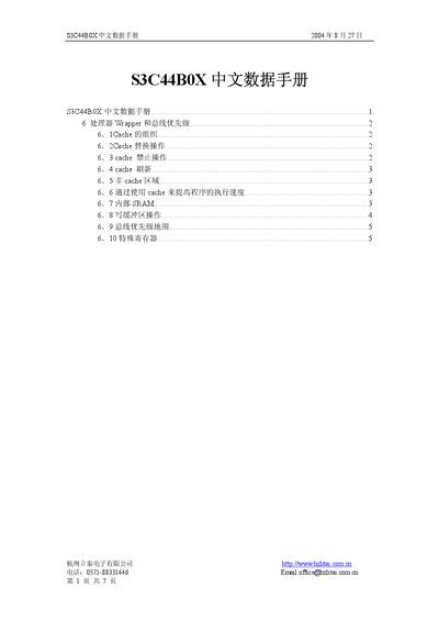
The S3C44B0X data manual describes the processor's internal architecture, including an 8 KB cache, internal SRAM, and a processor wrapper that manages cache, write buffer and bus arbitration. It explains how the cache can be configured, disabled, refreshed, and how non‑cache regions are defined for DMA and other operations.
The document also details the bus priority scheme for the seven bus masters (LCD_DMA, BDMA0/1, ZDMA0/1, nBREQ, and CPU wrapper) and lists the special registers (SYSCFG, NCACHBE0/1, SBUSCON) used to control cache mode, write buffer, and priority settings. This manual is written in Chinese.
| Cache size | 8 KB |
|---|---|
| Internal SRAM size | 8 KB (minimum) |
| Number of cache sets | 4 (set0‑set3) |
| Write buffer registers | 4 registers |
| Bus masters | 7 masters |
| Non‑cache region block size | 4 KB |
The processor provides four cache sets, labeled set0 through set3.
The internal SRAM is at least 8 KB in size.
The device supports seven bus masters, including LCD_DMA, BDMA0/1, ZDMA0/1, nBREQ, and the CPU wrapper.