
Key facts
Start here
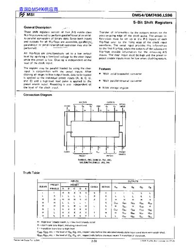
MSI DM54/DM7496, LS96 Shift Register Datasheet
This document provides technical specifications for the MSI DM54/DM7496 and LS96 series of 5-bit shift registers. These devices consist of five R-S master-slave flip-flops designed to perform parallel serial or serial-to-parallel conversion of binary data.
The datasheet details electrical characteristics, switching parameters, logic diagrams, and timing sequences for operation at a supply voltage of 5V.
MSI DM54 specifications
| Organization | 16 words of four bits each |
|---|---|
| Access Time (DM54/74) | 36 ns typical |
| Power Dissipation (DM54/74) | 400 mW |
| Power Dissipation (DMs4L/74L) | 75 mW |
All MSI DM54 documents by type
Ratings, dimensions and ordering codes, for selection and design work.
Questions answered in these manuals
What operation modes are supported?
The device supports parallel-in/parallel-out or serial-in/serial-out operations.
How is the register cleared?
All flip-flops are set to a low output level by applying a low-level voltage to the clear input while the preset is low.
What is the operation when Memory Enable is logical '0' and Write Enable is logical '1'?
Information applied to the four Write inputs will be written into the addressed location.
What is the operation when Memory Enable is logical '0' and Write Enable is logical '1'?
Information will be read as the complement of what was written into the memory.