
Key facts
- Model
- IDT74FCT533T
- Industry
- Industrial
- Documents
- 2
- Languages
- EN
- Last added
- 2012-06-05
Start here
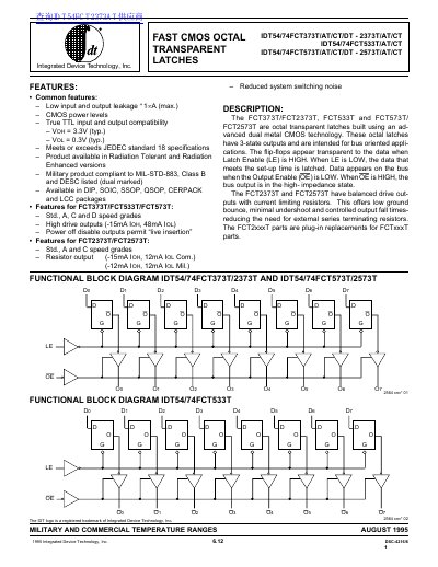
Integrated Device Technology Inc IDT54/74FCT373T/AT/CT/DT - 2373T/AT/CT IDT54/74FCT533T/AT/CT
This document is a product datasheet for the IDT54/74FCT373T, IDT54/74FCT2373T, IDT54/74FCT533T, and IDT54/74FCT573T series of fast CMOS octal transparent latches. These devices are built using advanced dual metal CMOS technology and feature 3-state outputs intended for bus-oriented applications.
Read onlineIntegrated Device Technology IDT74FCT533T specifications
| Technology | advanced dual metal CMOS technology |
|---|---|
| Output Type | 3-state outputs |
| Input Leakage (Max) | 1µA |
| Output HIGH Voltage (Typ) | 3.3V |
| Operating Temperature (Commercial) | 0 to +70 °C |
| Power Dissipation | 0.5 W |
Source: Integrated Device Technology Inc IDT54/74FCT373T/AT/CT/DT - 2373T/AT/CT IDT54/74FCT533T/AT/CT
All Integrated Device Technology IDT74FCT533T documents by type
Ratings, dimensions and ordering codes, for selection and design work.
Questions answered in these manuals
What is the function of the LE pin?
The Latch Enable (LE) input is active HIGH; when it is HIGH, the flip-flops appear transparent to the data.
From: Integrated Device Technology Inc IDT54/74FCT373T/AT/CT/DT - 2373T/AT/CT IDT54/74FCT533T/AT/CT
What happens when the OE pin is HIGH?
When Output Enable (OE) is HIGH, the bus output enters a high-impedance state.
From: Integrated Device Technology Inc IDT54/74FCT373T/AT/CT/DT - 2373T/AT/CT IDT54/74FCT533T/AT/CT
What are the input voltage levels for a logic HIGH and LOW?
A logic HIGH is guaranteed at 2.0 V or higher, and a logic LOW is guaranteed at 0.8 V or lower.
What is the quiescent power‑supply current of the device?
The quiescent current is about 0.01 mA under typical conditions.