
Key facts
- Brand
- EMLSI
- Model
- EM620FV16B
- Industry
- Industrial
- Documents
- 3
- Languages
- EN
- Last added
- 2012-06-11
Start here
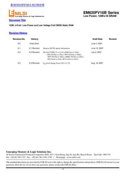
EMLSI EM620FV16B Series Low Power SRAM Datasheet
This document is a technical datasheet for the EMLSI EM620FV16B Series, which are Low Power, 128Kx16 SRAM devices manufactured using 0.15um Full CMOS technology. The chips feature three-state outputs compatible with TTL logic and are available in various speed grades including 45ns, 55ns, and 70ns.
The datasheet provides comprehensive specifications for the device, covering absolute maximum ratings, recommended DC operating conditions, and detailed AC timing parameters for both read and write cycles. It also includes information on packaging options such as chip trays and jar packing for wafer delivery.
EMLSI EM620FV16B specifications
| Organization | 128K x 16 |
|---|---|
| Process Technology | 0.15.um Full CMOS |
| Power Supply Voltage | 2.7~3.6V |
| Low Data Retention Voltage | 1.5V |
| Operating Temperature Range | -40 to 85 °C |
| Maximum Power Dissipation | 1.0 W |
All EMLSI EM620FV16B documents by type
Ratings, dimensions and ordering codes, for selection and design work.
Questions answered in these manuals
What is the minimum voltage for data retention?
The low data retention voltage is 1.5V.
Are these devices TTL compatible?
Yes, the device features three-state output and is TTL Compatible.
What supply voltage range does the EM620FV16B support?
The device operates from 2.7 V to 3.6 V.
What is the maximum power dissipation allowed for the EM620FV16B?
The absolute maximum power dissipation is 1.0 W.
What supply voltage range does the EM620FV16B support?
The device operates from 2.7 V to 3.6 V.
What is the allowed operating temperature range?
It can be used from –40 °C up to 85 °C.