
Data sheet for National Semiconductor DS75160A, DS75161A, and DS75162A high‑speed IEEE‑488 GPIB transceivers.
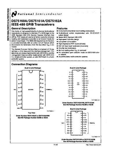
The DS75160A/DS75161A/DS75162A family provides 8‑channel bi‑directional transceivers that interface TTL/MOS logic to the IEEE‑488 GPIB bus. Features include internal bus termination, low power consumption, and selectable open‑collector mode for multi‑controller systems.
The document lists absolute maximum ratings, electrical and switching characteristics, connection diagrams, functional descriptions, logic diagrams, and timing waveforms, enabling designers to integrate these devices into instrumentation systems.
| Supply Voltage (Vcc) – max | 7.0 V |
|---|---|
| Input Voltage – max | 5.5 V |
| Storage Temperature Range | -65°C to +150°C |
| Operating Supply Voltage | 4.75 V to 5.25 V |
| Typical Input Hysteresis | 500 mV |
| High‑Level Input Voltage (V_H) | 2 V |
| Low‑Level Input Voltage (V_L) | 0.8 V |
| Output Low Current (Bus) | 48 mA |
The absolute maximum supply voltage is 7.0 V.
Typical input hysteresis is 500 mV.
They can be stored from –65 °C up to +150 °C.
The devices operate with a supply voltage between 4.75 V and 5.25 V.