
Demo manual for the Linear Technology DC185 demonstration board using the LT1370 6A switch regulator.
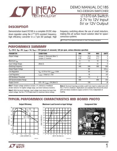
DC185 is a demonstration board for the LT1370 switching regulator. The manual covers its performance summary, typical performance characteristics, board photo, package and schematic diagrams, parts list, operation, components, thermal considerations, and PCB layout.
The board uses the LT1370 constant frequency converter in a 7-pin DD package. Hook-up instructions, component notes for the inductor, capacitors, snubber, and diodes, and PCB fabrication details are also included.
| Output voltage (J1 removed) | 11.6 / 12.0 / 12.4 V |
|---|---|
| Output voltage (J1 inserted) | 4.85 / 5.00 / 5.17 V |
| Maximum switch current | 6 / 8 / 10 A |
| Input voltage range | 2.7 to 12 V |
| Switching frequency | 440 to 580 kHz (typical 500 kHz) |
| Output ripple voltage | 80 mV P-P |
| Line regulation | 20 mV |
| Load regulation | 18 mV |
| S/D shutdown threshold | 0.6 to 2 V (typical 1.3 V) |
| S/D synchronization range | 600 to 800 kHz |
| Supply current | 100 µA typical |
| LT1370 input supply range | 2.7 to 30 V (DC185 maximum 12 V) |
| LT1370 quiescent current | 4.5 mA |
| LT1370 switch current | 6 A minimum |
| LT1370 switch on-resistance | 0.065 Ω typical |
| LT1370 switch breakdown voltage | 35 V minimum |
| LT1370 switching frequency | 500 kHz fixed |
| LT1370 shutdown supply current | 40 µA maximum |
| LT1370 reference voltage | 1.245 V |
| LT1370 negative feedback voltage | -2.48 V |
| LT1370 VC pin voltage | 1 V to 1.9 V |
| Inductor | 6.8 µH, 20% |
| Inductor saturation current | 5 A |
| Output voltage setting | VOUT = VREF (1 + R2/R1) |
It is intended for evaluating the LT1370 switching regulator in a typical step-up application.
The output voltage is set by R1 and R2, where VOUT = VREF (1 + R2/R1).
The board uses a BH Electronics 501-0726 6.8 µH inductor.
Use two or more capacitors in parallel instead of a larger value capacitor.