
This datasheet describes the PI6CB33201, a two-output very-low-power PCIe Gen1/Gen2/Gen3/Gen4/Gen5 clock buffer with on-chip termination and SMBus…
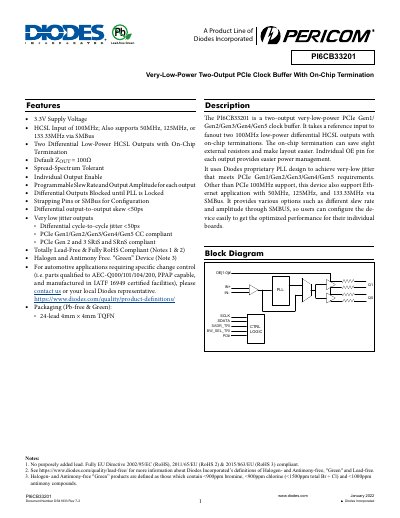
The PI6CB33201 is a two-output very-low-power PCIe Gen1/Gen2/Gen3/Gen4/Gen5 clock buffer designed to fanout a reference input into two 100MHz low-power differential HCSL outputs with on-chip terminations. This feature saves external resistors and simplifies layout.
The device utilizes Diodes Incorporated's proprietary PLL design to achieve very-low jitter that meets PCIe Gen1 through Gen5 compliance requirements. It supports Ethernet applications via SMBus at frequencies of 50MHz, 125MHz, and 133.33MHz, allowing users to configure slew rate and output amplitude for optimized board performance.
| Supply Voltage | 3.3V |
|---|---|
| Input Frequency (PCIe) | 100MHz |
| Output Type | Two Differential Low-Power HCSL Outputs with On-Chip Termination |
| Default Output Impedance | 100Ω |
| Output-to-Output Skew | <50ps |
| Cycle-to-Cycle Jitter | <50ps |
| Compliance | PCIe Gen1/Gen2/Gen3/Gen4/Gen5 CC compliant |
| RoHS Status | Totally Lead-Free & Fully RoHS Compliant |
The device supports PCIe Gen1, Gen2, Gen3, Gen4, and Gen5 compliance.
It includes on-chip termination which can save eight external resistors.