
This datasheet details the PI6CG18201, a very low power 2-output PCIe Gen1-4 clock generator with on-chip termination and programmable slew rate.
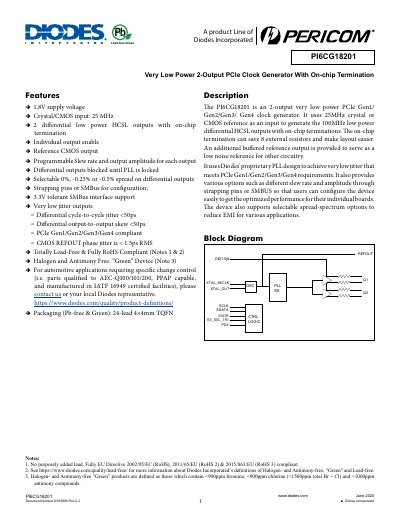
The PI6CG18201 is an integrated circuit designed as a 2-output very low power PCIe Gen1/Gen2/Gen3/Gen4 clock generator. It utilizes a 25 MHz crystal or CMOS reference input to generate 100 MHz differential HCSL outputs featuring on-chip termination, which eliminates the need for external resistors and simplifies PCB layout.
| Supply Voltage | 1.8V (nominal) |
|---|---|
| Output Type | Differential HCSL with on-chip termination |
| PCIe Compliance | Gen1/Gen2/Gen3/Gen4 |
| Jitter (Differential cycle-to-cycle) | <50ps |
| Output Skew | <50ps |
| Reference Output Jitter | < 1.5ps RMS |
| Operating Temperature Range (Industrial) | -40 to +85 °C |
The device accepts a crystal or CMOS reference input at 25 MHz.
Yes, it offers selectable options of 0%, -0.25%, or -0.5% spread on differential outputs.
Configuration can be performed using strapping pins or an SMBus interface.