
This guide explains the BL0937 chip's features, pinout, calibration method, energy‑measurement principle, BOM and PCB design tips.
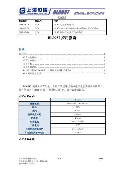
The BL0937 is a compact SOP‑8 chip designed for energy measurement in smart‑socket applications. It offers a wide measurement range, low power consumption and simple external circuitry.
The document provides detailed pin descriptions, calibration procedures, formulas for converting pulse frequencies to power, a parts list and practical PCB layout recommendations to ensure accurate measurements and reliable operation. This manual is written in Chinese.
| Measurement range | 5 mA ~ 20 A (1 W ~ 2500 W) |
|---|---|
| Power consumption | 1.7 mA |
| Signal response time | <300 ms |
| Startup current | 2 mA |
| Operating voltage | 3.3 V |
| Voltage drop protection | 2.7 V ± 50 mV |
| Effective‑value switch wait time | <10 µs |
| VDD pin voltage | +3.3 V (3.0 V ~ 3.6 V normal) |
| IP/IN differential voltage | ±50 mV |
| VP differential voltage | ±200 mV |
| CF1 pulse width | 38 µs (frequency proportional to power) |
Use a single‑point calibration: apply a rated voltage and current, measure the corresponding CF, CF1 and P pulse frequencies, then compute voltage, current and power conversion coefficients (Ku, Ki, Kp) for use in the system software.
CF1 provides an active‑power high‑frequency pulse with a fixed 38 µs width; its frequency is proportional to the measured power, and it also indicates over‑current with a 6.78 kHz pulse.
Place current‑sampling resistors and capacitors as close to the BL0937 pins as possible, keep differential traces short and parallel, use wide traces for the high‑current sampling resistor, separate the sampling ground from the power ground, and keep voltage‑sampling network away from current‑sampling lines.