
Demo manual for the Analog Devices DC2585A demonstration circuit featuring two LTC3290 high voltage boost charge pump circuits.
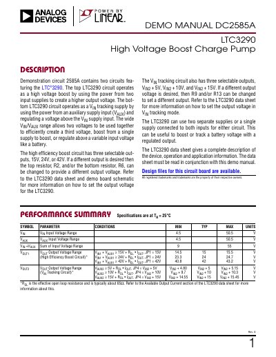
The DC2585A demonstration circuit contains two circuits featuring the LTC3290. The top circuit operates as a high voltage boost using power from two input supplies to create a higher output voltage, while the bottom circuit operates as a VIN tracking supply using an auxiliary supply input and regulating a voltage above the VIN supply input.
The wide VIN/VAUX range allows two voltages to be used together to efficiently create a third voltage, boost from a single supply, or regulate above a variable input voltage. The manual includes a performance summary, typical applications, assembly and test procedure, quick start procedure, operating equations, and parts list.
| VIN input voltage range | 4.5 V to 50.5 V |
|---|---|
| VAUX input voltage range | 4.5 V to 50.5 V |
| VIN + VAUX input voltage range | 9 V to 55 V |
| High efficiency boost selectable outputs | 15 V, 24 V, or 42 V |
| VIN tracking selectable outputs | VIN2 + 5 V, VIN2 + 10 V, or VIN2 + 15 V |
| Typical effective open-loop resistance (ROL) | about 65 Ω |
The high efficiency boost circuit has three selectable outputs: 15 V, 24 V, or 42 V.
The VIN tracking circuit has three selectable outputs: VIN2 + 5 V, VIN2 + 10 V, and VIN2 + 15 V.
Move JP1 to the desired VOUT1 selection or replace R2 and/or R6.
The typical ROL is about 65 Ω.