
This circuit note describes the interface between the AD9122 TxDAC and ADL5375-05 I/Q modulator, including design, schematic, and layout.
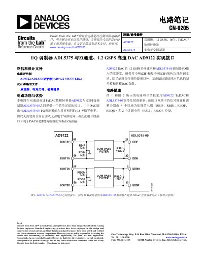
This document details a laboratory circuit design for interfacing the dual-channel, 1.2 GSPS, 16-bit TxDAC AD9122 with the broadband I/Q modulator ADL5375-05. The design supports both zero-IF and complex-IF architectures and includes a complete evaluation board design (AD9122-M5375-EBZ).
The note provides specific guidance on signal biasing, gain matching, and filtering. It describes the use of 50 Ω grounding resistors for biasing and recommends specific filter topologies, such as a 300 MHz fifth-order Butterworth filter, to suppress Nyquist images and spurs. Additionally, it covers level shifting techniques for driving the ADL5375-15 variant and offers layout recommendations to ensure signal integrity. This manual is written in Chinese.
| DAC Sampling Rate | 1.2 GSPS |
|---|---|
| Modulator Type | Broadband I/Q Modulator |
| Recommended Filter Bandwidth | 300 MHz |
| Filter Order | Fifth-order Butterworth |
| Bias Voltage (ADL5375-05) | 500 mV |
| Bias Voltage (ADL5375-15) | 1500 mV |
No, because the DAC output and the ADL5375-05 I/Q modulator input share the same 0.5 V bias level, so no active or passive level conversion circuit is needed.
For most applications, a value of 100 Ω is recommended, which results in a full-scale signal level of 1 V p-p.