
The ADCLK946 is an ultrafast SiGe clock fanout buffer with six LVPECL outputs and low‑jitter performance.
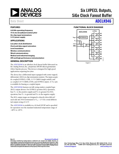
The ADCLK946 clock fanout buffer, fabricated on Analog Devices' XFCB3 SiGe bipolar process, provides six full‑swing LVPECL outputs for high‑speed clock distribution. It supports a wide range of input standards (LVPECL, CML, CMOS, LVDS) and includes on‑chip terminations and a VREF pin for biasing ac‑coupled inputs.
The device is supplied in a 24‑lead LFCSP package (4 mm × 4 mm) and operates over an industrial temperature range of –40 °C to +85 °C. Detailed specifications, pin descriptions, PCB layout guidelines, and termination options are provided for designers.
| Maximum Operating Frequency | 4.8 GHz |
|---|---|
| Broadband Random Jitter | 75 fs rms |
| Input Voltage High Level (VIH) | VEE + 1.6 VCC |
| Output Voltage High Level (VOH) Typical | VCC − 1.26 V |
| Supply Voltage Requirement (VCC‑VEE) Typical | 3.63 V |
| Positive Supply Current (IVCC) Typical | 275 mA |
The device can operate up to 4.8 GHz.
Typical broadband random jitter is 75 fs rms.
It requires a 3.3 V supply (typical 3.63 V, ±10%).