
TC74LCX32F/FN/FT/FK is a low-voltage quad 2-input OR gate from Toshiba. It features low-voltage operation (VCC = 1.65 to 3.6 V) and is compatible with 5-V supply environment for inputs.
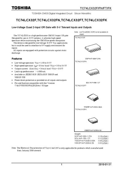
The TC74LCX32F is a low‑voltage CMOS quad 2‑input OR gate designed for 3.3 V systems but tolerant to 5 V inputs. It offers high‑speed propagation (tpd = 5.5 ns max) and low power dissipation, with protection against static discharge on all pins.
The device is supplied in multiple package types (JEDEC SOP, JEITA SOP, TSSOP, VSSOP) and includes power‑down protection on inputs and outputs. Absolute maximum ratings, operating ranges, and detailed electrical characteristics are provided for reliable circuit design.
| Supply voltage (Voc) range | 1.65 V to 3.6 V |
|---|---|
| Propagation delay (tpd) | 5.5 ns (max) |
| Output current (|IloH|/IloL) | 24 mA (min) |
| Latch‑up current capability | > 500 mA |
| Power dissipation (Pp) | 180 mW |
| Storage temperature range | -65 °C to 150 °C |
| Operating temperature range | -40 °C to 85 °C |
| Input diode current | ±50 mA |
| Output diode current | ±50 mA |
| Package options | JEDEC SOP, JEITA SOP, TSSOP, VSSOP |
It operates with a supply voltage (Voc) from 1.65 V to 3.6 V.
The maximum propagation delay is 5.5 ns.
JEDEC SOP, JEITA SOP, TSSOP, and VSSOP packages are available.
The device can dissipate up to 180 mW.