
SSM3J111TU is a Toshiba field effect transistor with fast switching, low power consumption, low on-resistance, and is suitable for power management switching circuits.
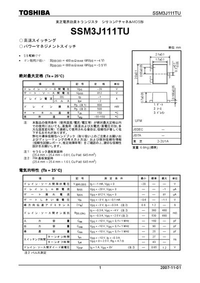
The SSM3J111TU is a silicon P‑channel MOSFET designed for high‑speed switching and power‑management applications. The document lists its absolute maximum ratings, typical on‑resistance, and voltage limits, and includes notes on safe operating conditions.
Detailed electrical parameters such as drain‑source voltage, on‑resistance, gate leakage, and switching times are presented, along with recommended PCB layout dimensions for both ceramic and FR‑4 substrates. Handling precautions emphasize electrostatic discharge protection and compliance with RoHS and export regulations. This manual is written in Japanese.
| Drain‑Source Voltage (VDS) max | -20 V |
|---|---|
| On‑Resistance (RDS(on)) max @ VGS = -4 V | 480 mΩ |
| Gate Leakage Current (IGSS) max | 1 µA |
The maximum drain‑source voltage is -20 V.
When handling the device, electrostatic discharge protection must be taken, such as using a grounded workbench and antistatic tools.