
TB6561NG is a dual bridge driver IC for DC motors, which uses DMOS elements as output transistors. It has low ON resistance and adopts PWM drive mode, enabling high power efficiency driving.
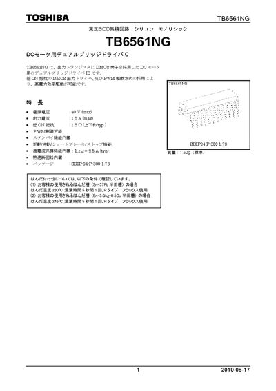
The TB6561NG is a dual‑bridge driver IC for DC motor control that uses DMOS output transistors for low ON resistance and PWM operation, enabling high‑efficiency power delivery. It supports supply voltages up to 40 V, output currents up to 1.5 A, and includes built‑in standby, over‑current protection and thermal shutdown functions.
The document provides a block diagram, pin configuration, electrical characteristics, PWM control details, over‑current detection circuitry, and example application circuits. It also contains mechanical dimensions, handling notes, and safety guidelines for proper integration into motor driver designs. This manual is written in Japanese.
| Maximum supply voltage (VCC) | 40 V (max) |
|---|---|
| Maximum output current | 1.5 A (max) |
| Typical ON resistance | 1.5 Ω (typ) |
| Operating temperature range | -20 °C to 85 °C |
| Input voltage range | -0.3 V to 5.5 V |
The device can be powered with up to 40 V on the VCC pin.
It can deliver up to 1.5 A per bridge channel.
Yes, it has built‑in over‑current protection (typical limit 2.5 A) and a thermal shutdown circuit.
The IC accepts 0‑5 V PWM signals on dedicated PWM pins for speed control.