
The HMC322 is a broadband non-reflective GaAs MESFET SP8T switch chip that covers a frequency range of DC to 10.0 GHz. It offers high isolation and low insertion loss, extending the frequency coverage of Hittite's SP8T switch product line. The switch includes an on-board binary decoder circuit, reducing the required logic control lines to three. It operates using a negative control voltage of 0/-5V and requires a fixed bias of -5V. All data is tested with the chip in a 50 Ohm test fixture connected via 0.025 mm (1 mil) diameter wire bonds of 0.5 mm (20 mils) length.
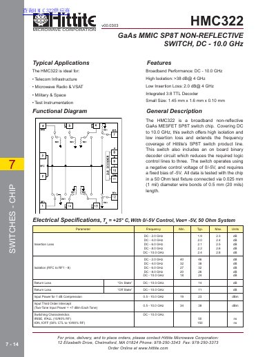
The HMC322 is a broadband non-reflective GaAs MESFET SP8T switch chip from Hittite Microwave Corporation covering DC to 10.0 GHz. It includes an on-board binary decoder circuit that reduces the required logic control lines to three, and it operates from a 0/-5V control voltage with a fixed -5V bias. The die measures 1.45 mm x 1.6 mm x 0.10 mm.
This six-page datasheet gives the electrical specifications measured with the chip in a 50 Ohm test fixture, plots of insertion loss, isolation, return loss and compression point, the truth table and control voltage table, absolute maximum ratings, an outline drawing, pad descriptions, and notes on handling, die mounting and wire bonding. Typical applications listed are telecom infrastructure, microwave radio and VSAT, military and space, and test instrumentation.
| Frequency Range | DC - 10.0 GHz |
|---|---|
| Isolation | >38 dB at 4 GHz |
| Insertion Loss | 2.0 dB at 4 GHz |
| Control Logic | Integrated 3:8 TTL decoder; three control lines A, B, C |
| Control Voltage | 0/-5V negative control; fixed bias of -5V |
| Bias Voltage (Vee) | -5.0 Vdc ± 10% |
| Operating Temperature | -40 to +85 °C |
| Storage Temperature | -65 to +150 °C |
| Die Size | 1.45 mm x 1.6 mm x 0.10 mm |
| Switching Characteristics | tRISE/tFALL 50 ns; tON/tOFF 150 ns |
It is a broadband non-reflective GaAs MESFET SP8T switch chip that covers DC to 10.0 GHz.
Three, because the chip includes an on-board binary decoder circuit that reduces the required logic control lines to three.
A Vee range of -5.0 Vdc ± 10%, with typical Iee of 5.0 mA and maximum Iee of 9.0 mA.
Handle the chip in a clean environment, follow ESD precautions against > ± 250V strikes, suppress transients, and handle it along the edges with a vacuum collet or bent tweezers.