
This document is the EMIF08-VID01F2 datasheet, the device is an 8-line highly integrated device designed to suppress EMI/RFI noise in all systems subjected to electromagnetic interference. This device has high efficiency EMI filter(-33 dB @ 900 Mhz), low line capacitance(suitable for high speed data bus), low series resistance(suitable for camera impedance matching), optimized PCB space consuming(1.29 mm x 3.92 mm), very thin package(0.65 mm), lead free package, high efficiency of ESD suppression(IEC61000-4-2 level 4), high reliability provided by monolithic integration, high reduction of parasitic elements through integration and wafer level packaging.
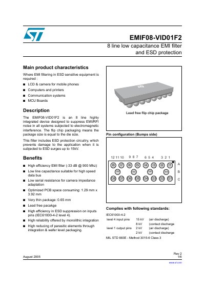
The EMIF08-VID01F2 is a highly integrated 8-line device designed to suppress EMI/RFI noise in systems subjected to electromagnetic interference. It features flip chip packaging with dimensions of 1.29 mm x 3.92 mm and includes built-in ESD protection circuitry capable of handling surges up to 15kV.
| ESD discharge (contact) | 8 KV |
|---|---|
| Maximum junction temperature | 125 C |
| Operating temperature range | -40 to +85 C |
| Series resistance between Input & Output | 80 to 120 Ohms |
| Package type | Flip Chip |
The device withstands an IEC61000-4-2 air discharge of up to 15 kV on its input pins.
The filter has a typical line capacitance of 16 pF when measured at 3V.
The optimized PCB space consuming size is 1.29 mm x 3.92 mm with a thickness of 0.65 mm.