
STCD1020, STCD1030, STCD1040 are low-power, low-phase-noise multi-channel clock distribution circuits. They are available in 2, 3 or 4-output versions with single-ended sine or square-wave clock input and output. Each output has an independent clock enable, reducing clock source fanout. The input does not require AC coupling capacitors, making them ideal for multi-mode RF clock references and baseband peripherals clock references.
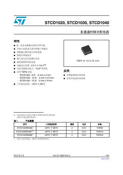
The STMicroelectronics STCD1020, STCD1030, and STCD1040 are single-supply unit-gain clock distribution circuits with 2, 3, or 4 outputs. They are designed to provide a common frequency clock for multi-mode mobile RF applications and can also serve as clock references for baseband peripherals such as WLAN, Bluetooth, GPS, and DVB-H in mobile phones.
These devices feature independent enable signals for each output buffer to reduce power consumption when the connected device does not require a clock. They operate with input and output single-ended sine or square wave clocks and are suitable for common mobile phone master clock frequencies ranging from 10 MHz to 52 MHz. This manual is written in Chinese.
The devices operate from -40°C to 85°C.
The TDFN-12 package measures 2 mm by 3 mm.