
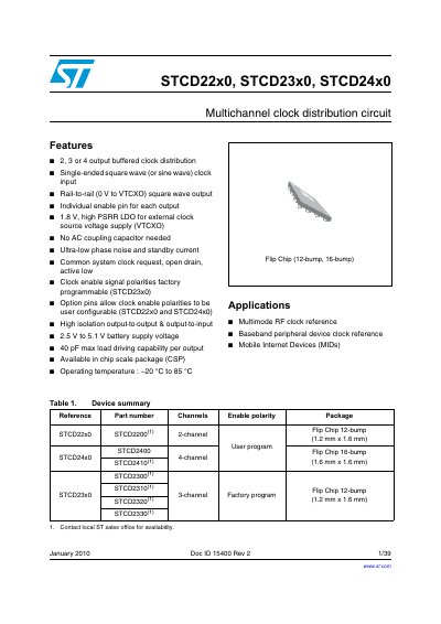
The STCD22x0, STCD23x0, and STCD24x0 are 2, 3, or 4 output buffered clock distribution circuits that accept external square wave or sine wave signals. They provide rail-to-rail square wave outputs and include a common system clock request feature to control an external clock source.
These devices integrate a 1.8 V high PSRR LDO for the external clock supply voltage, eliminating the need for AC coupling capacitors. Available in chip scale packages (CSP) with flip-chip bumps, they support battery supply voltages from 2.5 V to 5.1 V and operate over an industrial temperature range of -20 °C to +85 °C.
| Number of outputs | 2, 3 or 4 output buffered clock distribution |
|---|---|
| Input signal type | Single-ended square wave (or sine wave) |
| Output signal type | Rail-to-rail (0 V to VTCXO) square wave output |
| Supply voltage range | 2.5 V to 5.1 V |
| Operating temperature range | -20 °C to +85 °C |
| Max load driving capability per output | 40 pF |
The devices can be operated with an operating temperature ranging from -20 °C to +85 °C.
No, the STCD22x0, STCD23x0 and STCD24x0 do not need an AC coupling capacitor.
The devices support a battery supply voltage ranging from 2.5 V to 5.1 V.