
This datasheet describes the features of the OMNIFET II fully autoprotected Power MOSFET VNN7NV04P-E and VNS7NV04P-E, including linear current limitation, thermal shutdown, short circuit protection, integrated clamp, low input pin current, diagnostic feedback, ESD protection, direct access to the gate of the Power MOSFET (analog driving) and compatibility with standard Power MOSFET in compliance with the 2002/95/EC European Directive.
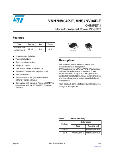
The VNN7NVO4P-E and VNS7NVO4P-E are monolithic OMNIFET II devices designed in STMicroelectronics VIPower™ MO0-3 Technology. They are intended for replacement of standard Power MOSFETs in DC up to 50 kHz applications. These devices feature built-in thermal shutdown, linear current limitation, and overvoltage clamp to protect the chip in harsh environments.
| Reverse DC output current | -10.5 A |
|---|---|
| Operating junction temperature | Internally limited |
| Storage temperature | -55 to 150 °C |
The device includes linear current limitation, thermal shutdown, short circuit protection, and an integrated clamp.
The maximum reverse DC output current is -10.5 A.