
ST8004 is a smart card interface designed to minimize the microprocessor hardware and software complexity in all the applications that need a smart card, such as Set-Top-Boxes, electronic payments, pay TV and identification. The ST8004 is compliant with the NDS requirements. It implements all the blocks and procedures for the card activation/deactivation as shown in the block diagram of figure 1.
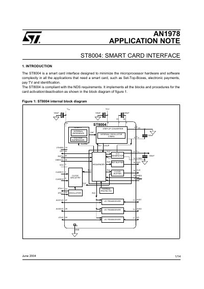
The document provides an introduction to the ST8004 smart card interface, which is designed to minimize microprocessor complexity in applications like set-top boxes and electronic payments. It details the internal block diagram and explains how the device coordinates enable signals for card activation and deactivation according to ISO/IEC 7816 standards.
Key sections cover clock signal generation using crystals or external signals, the operation of the internal step-up converter for driving 3V and 5V cards, and specific PCB design recommendations. The note also outlines fault detection capabilities, including over-temperature, card removal, under-voltage, and short-circuit protection.
The Vcc pin remains between 4.60V and 5.30V for Class-A cards, or between 2.7V and 3.3V for Class-B cards.
The wire should be less than 5cm long.
The application circuitry should ensure that the VDD voltage falls more slowly than 1.6V/ms.