
The AD5317R is a low drift 2.5V reference with 10-bit resolution and 2ppm/°C temperature drift, in a 3mm*3mm package.
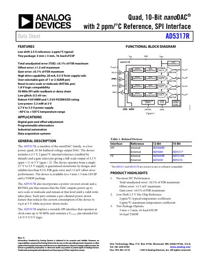
The AD5317R is a member of the nanoDAC family, functioning as a low power, quad, 10-bit buffered voltage output digital-to-analog converter (DAC). It features a built-in 2.5 V reference with a typical temperature coefficient of 2 ppm/°C and includes a gain select pin for full-scale outputs of either 2.5 V or 5 V.
The device operates from a single supply ranging from 2.7 V to 5.5 V and supports SPI clock rates up to 50 MHz. It incorporates power-on reset circuitry via the RSTSEL pin, ensuring outputs start at zero scale or midscale upon power-up. The AD5317R is available in a 3 mm x 3 mm LFCSP package and a TSSOP package.
| Resolution | 10 Bits |
|---|---|
| Total Unadjusted Error (TUE) | +0.1% of FSR maximum |
| Offset Error | +/- 1.5 mV maximum |
| Gain Error | +0.1% of FSR maximum |
| Supply Voltage Range | 2.7 V to 5.5 V |
| SPI Clock Rate | Up to 50 MHz |
| Reference Voltage | 2.5 V, 2 ppm/°C typical |
| Output Current Capability | 20 mA |
The internal 2.5 V reference has a typical temperature coefficient of 2 ppm/°C.
Yes, the device features 1.8 V/3 V/5 V logic compatibility.