
The RP502x series of synchronous rectifier step-down DC/DC converters are based on the CMOS process. They contain an oscillator, a reference voltage unit, an error amplifier, a switching control circuit, a soft-start circuit, protection circuits, an UVLO circuit, and switching transistors. Using built-in switch transistors for synchronous rectification, a high-efficiency step-down DC/DC converter is composed of only an inductor and capacitors. As protection circuits, the ICs contain a current limit circuit and a latch protection circuit. The current limit circuit controls the peak current of LX at each clock cycle. If the load current exceeds the limit value for a certain period of time, the latch protection circuit maintains the built-in driver in OFF state. To cancel the latch protection, disable the ICs with a chip enable circuit and then enable it again, or make the power supply voltage lower than UVLO. The setting voltage for the RP502x series is the output voltage fixed type with built-in feedback resistance that is adjustable in 0.1V step with the accuracy of ± 1.5% or ±24mV. The packages for the ICs are WLCSP-6-P2 and DFN1616-6, which enable the high-density mounting. The switching mode for the ICs is selectable from the PWM/VFM auto switching type, which achieves the high efficiency at the light load condition or PWM fixed type, which switches at the fixed frequency.
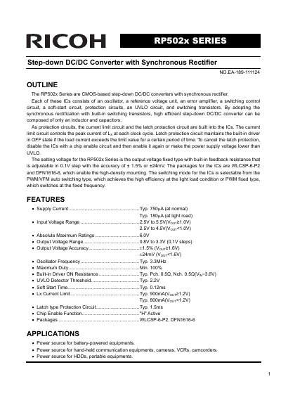
The RP502x Series are CMOS-based step-down DC/DC converters featuring a built-in synchronous rectifier to achieve high efficiency. The ICs integrate an oscillator, reference voltage unit, error amplifier, switching control circuit, soft-start circuit, and various protection circuits including current limit and latch protection.
These devices offer adjustable output voltages in 0.1V steps with an accuracy of +1.5% or +24mV. The switching mode is selectable between PWM/VFM auto switching for high efficiency at light loads and a fixed-frequency PWM type. Available packages include WLCSP-6-P2 and DFN1616-6, enabling high-density mounting.
| Supply Current (Typical) | 750uA (at normal), 180uA (at light load) |
|---|---|
| Output Voltage Range | 0.8V to 3.3V (0.1V steps) |
| Oscillator Frequency | Typ. 3.3MHz |
| Maximum Duty Cycle | 100% |
| Built-in Driver ON Resistance (Typ.) | Pch. 0.5Ω, Nch. 0.5Ω |
| UVLO Detector Threshold (Typ.) | 2.2V |
| Soft Start Time (Typ.) | 0.12ms |
| Lx Current Limit (Typ.) | 900mA (Vout>=1.2V), 800mA (Vout<1.2V) |
| Latch Protection Circuit Delay (Typ.) | 1.5ms |
| Chip Enable Function | 'H' Active |
The output voltage accuracy is +1.5% for voltages greater than or equal to 1.6V, and +24mV for voltages less than 1.6V.
The available packages are WLCSP-6-P2 and DFN1616-6.
The operating temperature range is -40 to 85 °C.