
This document describes the features and characteristics of ADG3248, which is a 2.5V/3.3V 2:1 multiplexer/demultiplexer with low delay, high speed, and low power dissipation.
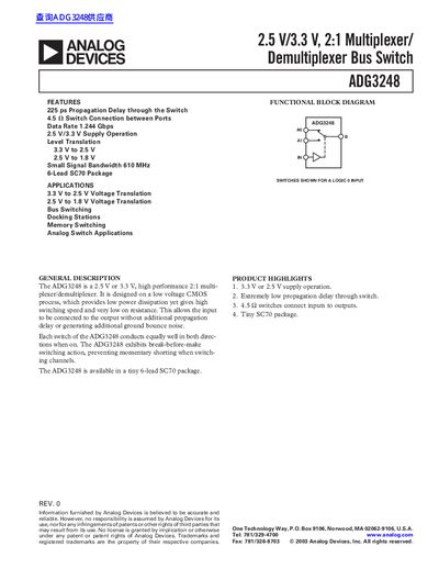
The ADG3248 is a high-performance 2:1 multiplexer/demultiplexer designed on a low voltage CMOS process. It supports both 2.5 V and 3.3 V supply operation, enabling level translation between these voltages as well as down to 1.8 V. The device features extremely low propagation delay of 225 ps through the switch.
| Propagation Delay through the Switch | 225 ps |
|---|---|
| Switch Connection between Ports | 4.5 Ω |
| Data Rate | 1.244 Gbps |
| Supply Operation | 2.5 V/3.3 V |
| Small Signal Bandwidth | 610 MHz |
| Package Type | 6-Lead SC70 |
| Operating Temperature Range (Industrial) | -40°C to +85°C |
The device supports 2.5 V or 3.3 V supply operation.
The maximum data rate is 1.244 Gbps.
It is available in a tiny 6-lead SC70 package.