
The ADG3249 is a 2.5V or 3.3V, high performance 2:1 multiplexer/demultiplexer bus switch. It is designed on a low voltage CMOS process, which provides low power dissipation yet gives high switching speed and very low on resistance. This allows the input to be connected to different voltage sources without any interference. The switch is available in a low power SOT-23 package.
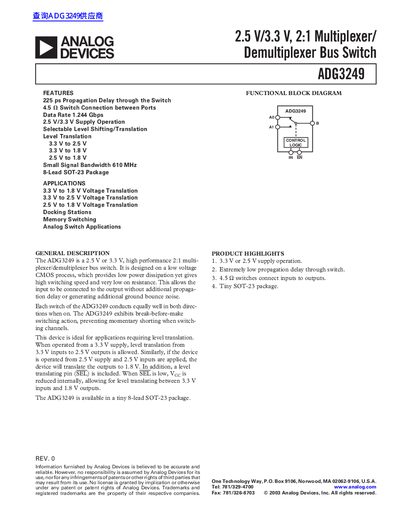
The ADG3249 is a high-performance 2:1 multiplexer/demultiplexer bus switch designed on a low voltage CMOS process. It operates from 2.5 V or 3.3 V supplies and features selectable level shifting/translation to convert between 3.3 V, 2.5 V, and 1.8 V logic levels.
| Propagation Delay through the Switch | 225 ps |
|---|---|
| Switch Connection Resistance | 4.5 Ω |
| Data Rate | 1.244 Gbps |
| Supply Operation Voltage | 2.5 V/3.3 V |
| Small Signal Bandwidth | 610 MHz |
| Package Type | 8-Lead SOT-23 |
| Operating Temperature Range (Industrial) | -40°C to +85°C |
The device supports translation from 3.3 V inputs to 2.5 V outputs, and from 2.5 V inputs to 1.8 V outputs.
Yes, when operated from a 3.3 V supply with the SEL pin low, it allows level translating between 3.3 V inputs and 1.8 V outputs.
The maximum data rate is 1.244 Gbps when operated with a 3.3 V supply.