
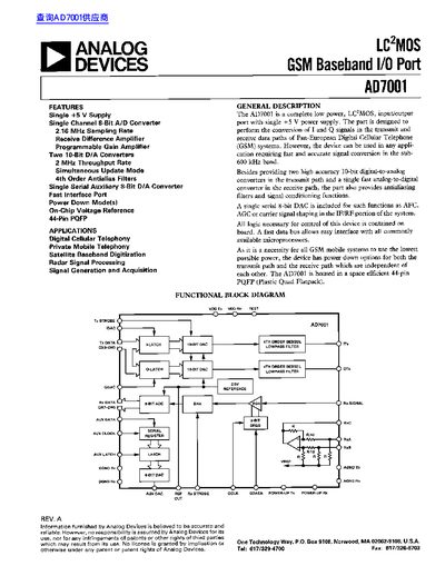
Analog Devices AD7001A GSM Baseband I/O Port Datasheet


Analog Devices AD7001A GSM Baseband I/O Port Datasheet - cover page
Brand
Analog Devices
Category
Other Electronics
Document type
Datasheet
Language
English
Pages
16
File format
PDF
File size
622 KB
Published
07 June, 2012
Updated
27 July, 2012
MD5 checksum
0181FB11D18CA7AEA46055FD5913AD02

About this manual

The AD7001 is a complete low power, LC MOS input/output port with single +5 V power supply. The part is designed to perform the conversion of I and Q signals in the transmit and receive data paths of Pan-European Digital Cellular Telephone (GSM) systems. However, the device can be used in any application requiring fast and accurate signal conversion in the sub-600 kHz band.

What's inside

  • Features
  • Applications
  • General Description
  • Specifications
  • Functional Block Diagram
  • Absolute Maximum Ratings
  • Pin Configuration
  • Ordering Guide

Specifications

Supply Voltage+5 V
ADC Resolution8 Bits
Sampling Rate2.17 MSPS
DAC Resolution10 Bits
Number of DAC Channels2

Frequently asked questions

What is the maximum sampling rate of the AD7001?

The device supports a sampling rate of 2.17 MSPS.

Does the AD7001 include an on-chip voltage reference?

Yes, it includes a Reference Output with a range of 2.4/2.6 V min/V max.

What is the power consumption when all sections are powered down?

The maximum current draw in this mode is 2.0 mA.

Download PDF (622 KB)

More Analog Devices Manuals


View all Analog Devices manuals →