
The AD7010 is a complete low power, CMOS, π/4 DQPSK modulator with single +5 V power supply. The part is designed to perform the baseband conversion of I and Q transmit waveforms in accordance with the Japanese Digital Cellular Telephone system. The on-chip π/4 Differential Quadrature Phase Shift Keying (DQPSK) digital modulator, which includes the Root Raised Cosine filters, generates I and Q data in response to the transmit data stream. The AD7010 also contains ramp control envelope logic to shape the I and Q output waveforms when ramping up or down at the beginning or end of a transmit burst. Besides providing all the necessary logic to perform π/4 DQPSK modulation, the part also provides reconstruction filters to smooth the DAC outputs, providing continuous time analog outputs. The AD7010 generates differential analog outputs for both the I and Q signals. As it is a necessity for all digital mobile systems to use the lowest possible power, the device is designed in a low power manner.
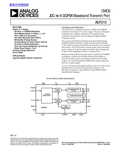
The document describes the AD7010, a complete low power CMOS 2/4 DQPSK modulator designed for baseband conversion in accordance with the Japanese Digital Cellular Telephone system. Key features include on-chip 7/4 DQPSK modulation, root-raised-cosine transmit filters, and two 10-bit D/A converters.
| Supply Voltage (VDD) | +5 V +/- 10% |
|---|---|
| Power Dissipation | 30 mW typical |
| Operating Temperature Range (Industrial) | -40°C to +85°C |
| Package Type | 24-pin SSOP |
It is designed to perform baseband conversion for the Japanese Digital Cellular Telephone system.
Yes, it includes Root-Raised-Cosine Tx Filters.
The maximum operating temperature is +85°C.