
This is a technical datasheet of Elpida Memory EDS6432AFBH, EDS6432CFBH 64M bits SDRAM
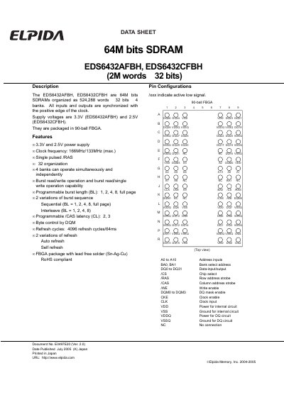
The EDS6432AFBH and EDS6432CFBH are 64‑Mbit SDRAMs organized as 2 M words × 32 bits with four independent banks. They operate with a single‑ended clock and support burst read/write operations.
Key features include selectable supply voltages (3.3 V or 2.5 V), maximum clock frequencies of 166 MHz/133 MHz, programmable burst lengths and CAS latencies, and a 90‑ball FBGA package that complies with RoHS.
| Supply Voltage | 3.3 V (AF) / 2.5 V (CF) |
|---|---|
| Maximum Clock Frequency | 166 MHz (AF) / 133 MHz (CF) |
| Organization | x32, 4 banks |
| Bank Operation | 4 banks can operate simultaneously and independently |
| Burst Length Options | 1, 2, 4, 8, full page |
| CAS Latency Options | 2, 3 |
| Package | 90‑ball FBGA, lead‑free Sn‑Ag‑Cu |
| Operating Temperature | 0 °C to +70 °C |
| Power Dissipation | 1.0 W |
The EDS6432AFBH operates at 3.3 V, while the EDS6432CFBH operates at 2.5 V.
The AF version supports up to 166 MHz and the CF version up to 133 MHz.
The SDRAM contains four banks that can operate simultaneously and independently.