
The HY57V561620T is a 268,435,456-bit CMOS Synchronous DRAM, ideally suited for main memory applications that require large memory density and high bandwidth. It is organized as 4 banks of 4,194,304 x 16 and offers fully synchronous operation with internally pipelined design for high bandwidth. It supports programmable options including CAS latency, burst length, and burst count sequence.
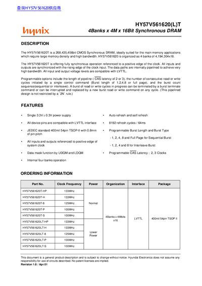
The HY57V561620(L)T is a 268,435,456‑bit CMOS synchronous DRAM organized as four banks of 4,194,304 × 16 bits. It operates with a single 3.3 V + 0.3 V power supply and supports LVTTL‑compatible I/O levels. The device offers programmable burst lengths, CAS latency options, and auto‑refresh capabilities.
The datasheet provides detailed pin configurations, functional block diagrams, absolute maximum ratings, DC and AC characteristics, command timing tables, and package dimensions for the 400 mil 54‑pin TSOP‑II package.
| Memory density | 268,435,456 bit |
|---|---|
| Organization | 4 banks of 4,194,304 × 16 |
| Power supply | 3.3 V + 0.3 V |
| Refresh cycles | 8192 cycles per 64 ms |
| Ambient temperature range | 0 °C to 70 °C |
| Input high voltage (VIH) | 2.0 V – 3.0 V (VDDQ + 0.3 V) |
| Package type | 400 mil 54‑pin TSOP‑II |
The device uses a single 3.3 V + 0.3 V power supply, with a typical operating range of 3.0 V to 3.6 V.
The absolute maximum ambient temperature is 0 °C to 70 °C.
It supports 8192 refresh cycles per 64 ms interval.
It is supplied in a 400 mil 54‑pin Thin Small Outline Package (TSOP‑II).