
This document describes the features and characteristics of the ESMT Preliminary M12L128168A chip.
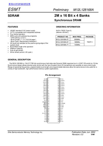
The ESMT M12L128168A is a 128‑Mbit synchronous DRAM organized as 4 banks of 2 M × 16‑bit words. The document provides an overview of its features, pin arrangement, block diagram, and functional description, as well as absolute maximum ratings and recommended operating conditions.
Key sections include detailed pin descriptions, timing parameters for different CAS latency settings, AC and DC characteristic tables, and packaging dimensions. The datasheet also contains safety notices and usage restrictions for critical applications.
| Capacity | 128 Mbit (2 M × 16 × 4 banks) |
|---|---|
| Package | 54‑lead TSOP (Type II) |
| Maximum Operating Frequency | 200 MHz (5T version) |
| Supply Voltage (typical) | 3.3 V |
| Supply Voltage Range | 3.0 V – 3.6 V |
| Storage Temperature Range | -55 °C to +150 °C |
| Power Dissipation | 1 W |
| Input Capacitance (per pin) | 2.5 pF – 4 pF |
| Data I/O Capacitance (DQ0‑DQ15) | 2 pF – 6.5 pF |
It uses a 54‑lead TSOP (Type II) package.
The recommended supply voltage is 3.0 V to 3.6 V, with a typical value of 3.3 V.
The 5T version can operate up to 200 MHz.
The device can be stored from –55 °C up to +150 °C.