
This datasheet provides the specifications of ESMT M52S128324A memory, including operating voltage, operating temperature, timing, etc.
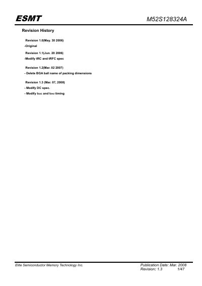
The M52S128324A is a 1 M × 32‑bit × 4‑bank synchronous DRAM that complies with JEDEC 2.5 V standards. It supports multiple CAS latencies, burst lengths, and special functions such as PASR and TCSR, making it suitable for high‑bandwidth memory systems.
The document provides detailed pin assignments, electrical characteristics, timing parameters, packaging dimensions for both TSOP‑II and FBGA options, and safety notices for critical applications. This manual is written in Chinese.
| Memory Capacity | 1 M × 32 bit × 4 Banks |
|---|---|
| Supply Voltage (VDD, VDDQ) | 2.3 V – 2.7 V |
| CAS Latency Options | 1, 2, 3 |
The recommended VDD and VDDQ range is 2.3 V to 2.7 V.
The SDRAM supports CAS latencies of 1, 2, or 3 clock cycles.