
LTC485 is a low power differential bus/line transceiver designed for multipoint data transmission standard RS485 applications with extended common mode range (12V to –7V). It also meets the requirements of RS422. CMOS design offers significant power savings over its bipolar counterpart without sacrificing ruggedness against overload of ESD damage. The driver and receiver feature three-state outputs, with the driver outputs maintaining high impedance over the entire common mode range. Excessive power dissipation caused by bus contention or faults is prevented by a thermal shutdown circuit which forces the driver outputs into a high impedance state. The receiver has a fail-safe feature which guarantees a high output state when the inputs are left open. The LTC485 is fully specified over the commercial and extended industrial temperature range.
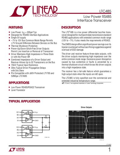
The LTC485 is a low‑power differential bus transceiver designed for RS485 and RS422 applications. It operates from a single 5 V supply, offers a common‑mode range of –7 V to +12 V, includes thermal‑shutdown protection, and provides glitch‑free driver outputs that can be live‑inserted or removed.
Typical applications include low‑power RS485/RS422 communication, level translation, and industrial data links where power consumption must be minimized. The device features three‑state driver and receiver outputs, fail‑safe operation, and can support up to 32 transceivers on a single bus.
| Supply Current (No Load, Outputs Enabled) | 500 pA typ |
|---|---|
| Receiver Input Hysteresis | 70 mV typ |
| Common‑Mode Voltage Range | -7 V to +12 V |
The typical no‑load supply current is 500 pA when the outputs are enabled.
It supports a common‑mode range from –7 V to +12 V.
The receiver input hysteresis is typically 70 mV.